Z80-Nexus a Z80 ROMless SBC
Repository: github.com/gloveboxes/Z80ROMlessSBC
Overview
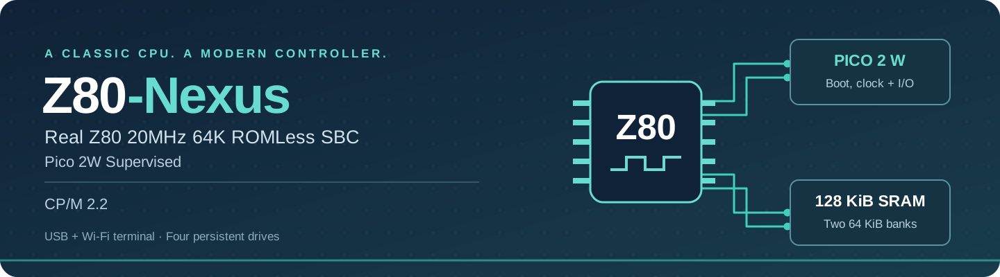
Z80-Nexus pairs a Z80 processor with a Raspberry Pi Pico 2 W to run CP/M without a ROM chip.
Who this project is for
For retro-computing enthusiasts who want to learn how agentic AI can support hardware and software design. Explore the full process: building and testing a computer, developing firmware and CP/M applications, and designing a PCB for manufacturing.
Start building
Install the software listed in Toolchain, including the complete Arm compiler, Python, Pico SDK and USB utilities.
- Check the parts inventory and read the breadboard and meter basics.
- Follow the implementation plan in order, from power checks through SRAM loading, CP/M, and terminal and disk testing.
- Use the firmware build and flashing guide to build and load the firmware for your current phase.
The hardware chapters are detailed references; you do not need to understand every firmware excerpt before starting. Use the glossary for unfamiliar terms.
How does it boot without ROM?
The Pico feeds the Z80 instructions that make it write and verify its own boot image in SRAM. After verification, the Z80 is reset and starts executing that image from RAM. The Pico never drives the memory address bus or writes SRAM directly.
See the loader sequence for the protocol and timing, and Phase 6 for the implementation and hardware checks.
System architecture
The Pico 2 W is a multicore I/O controller: core 0 configures the nominal 20 MHz Z80 clock and owns assisted SRAM loading and Z80 I/O. Phases 9 and 10 generate the clock and complete every Z80 I/O cycle in PIO, including SRAM bank selects. Core 1 owns USB, runtime storage, Wi-Fi and network clients. Bounded console rings and request/result mailboxes separate the two cores. The Z80 itself writes SRAM during loading and executes CP/M directly from SRAM after verification and reset. USB supervisor commands request Z80 actions through a bounded queue; USB interrupts and endpoint operations remain on core 1.
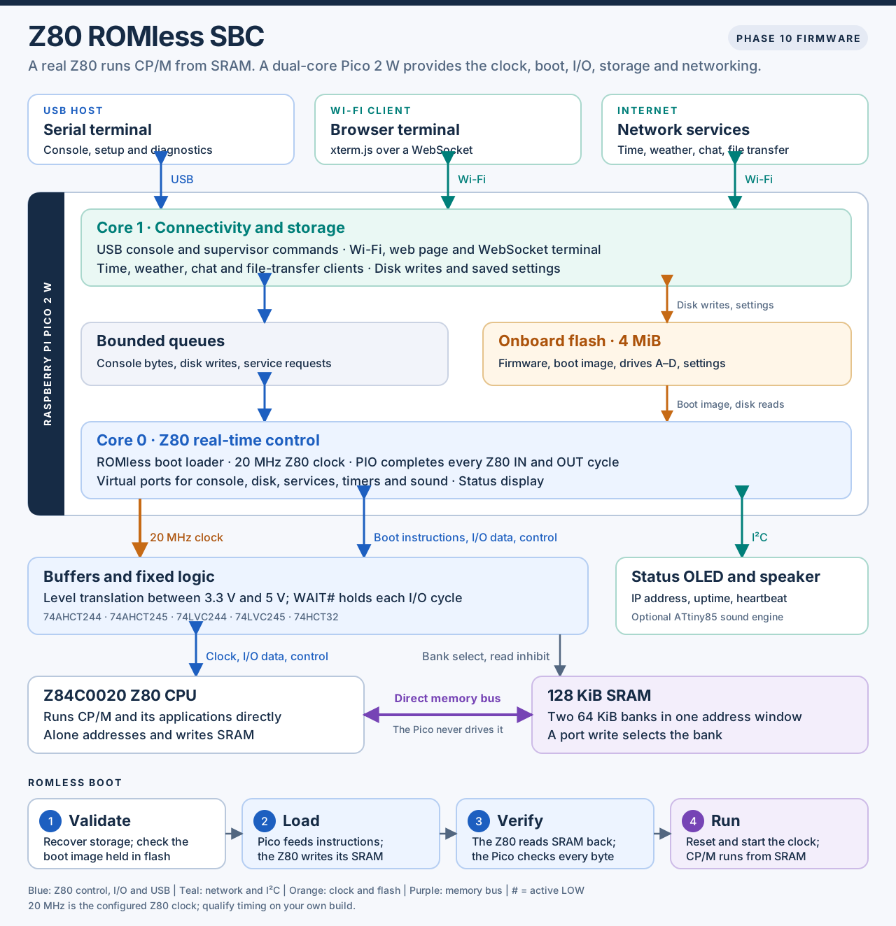
Open or download the full-size SVG. The diagram follows the maintained Phase 10 implementation, which compiles the Phase 9 automatic-loader application with networking enabled.
Working and tested breadboard implementation
The breadboard implementation shown below has been built and tested, running the Z80 at 20 MHz with CP/M executing from SRAM. It brings together the Z80, Pico 2 W, SRAM, and interface logic across three BB830 breadboards.
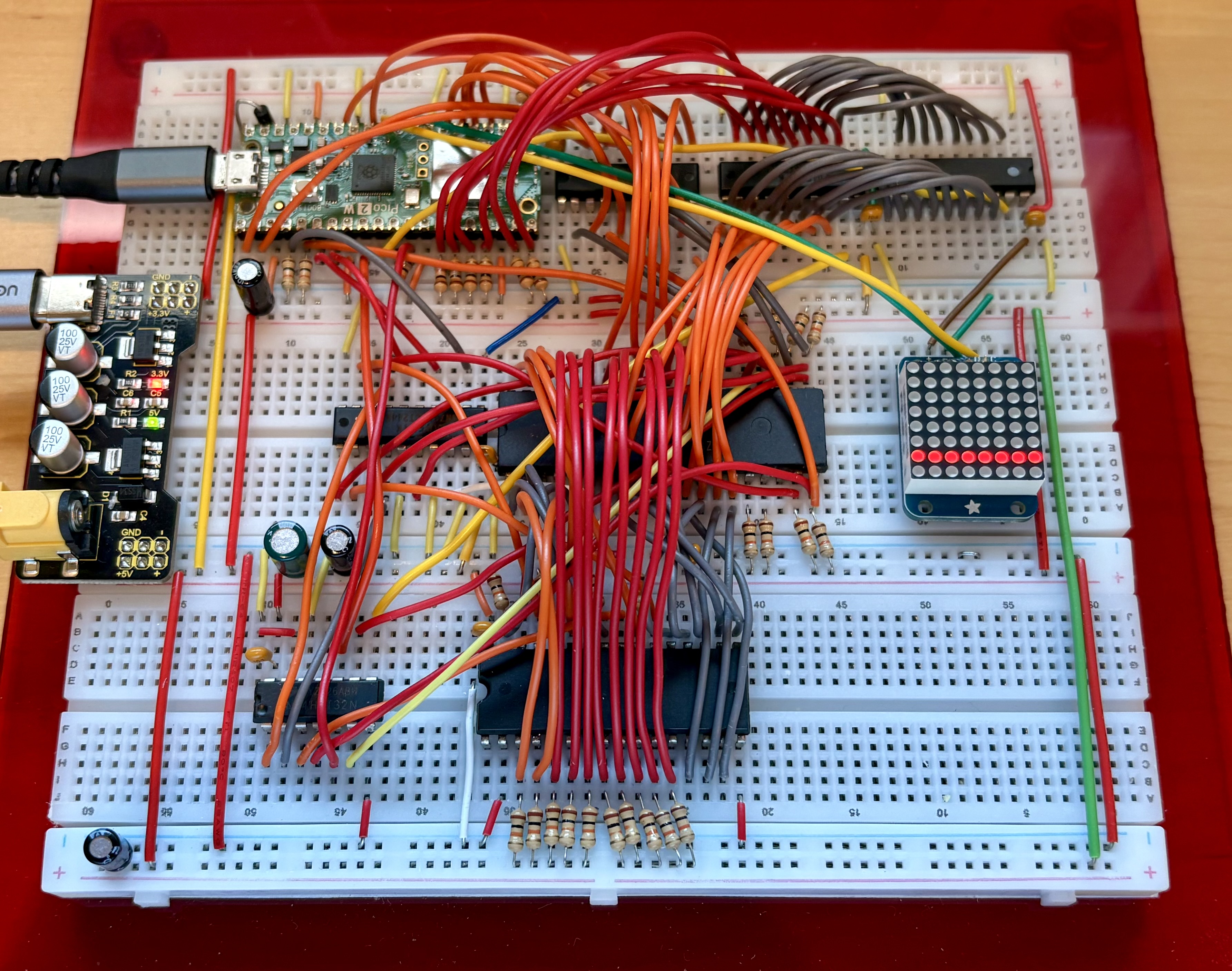
Follow the staged implementation plan to reproduce the build and validate each stage, from power and clock checks through ROMless boot loading, terminal access, and persistent disk I/O.
Explore further
- USB CP/M terminal and flash storage - load CP/M, reach the prompt, and test persistent disk I/O.
- System operation - virtual I/O, flash storage, and runtime coordination.
- I/O ports and services - the terminal and disk interface, plus ROMLESS-SVC/1 timers, clock, utilities and persistent environment variables.
- CP/M documentation - boot-image construction, disk media, and software compatibility.
- Firmware testing - host tests, Z80 emulation, and hardware validation boundaries.
- Pico flashing and USB supervisor tools - device selection, verified updates, clean stop, and journal diagnostics.
- Source index - maintained firmware, tools, and implementation guides.