3. Construction and Breadboard Topology
Build the phase sequence; leave later devices absent until instructed. Every pin map is a top view. Matching schematic net labels mean an electrical connection even without a continuous drawn wire.
Before You Wire
On each BB830, A-E at one numbered row are one connection; F-J at that row are a separate connection. The center ravine isolates them. Adjacent numbered rows are not connected. Check power-rail continuity with a meter: stripes do not prove internal continuity or voltage.
Wire one named source pin to one named destination pin, then check continuity at the actual socket contacts and shorts to adjacent contacts. GP2 is Pico header pin 4, not header pin 2. A0-A15 means sixteen independent nets. Strip only enough insulation to seat the jumper, with no exposed bridges.
Use the Meter Safely
Use resistance/continuity only with external power and USB disconnected and capacitors discharged. Do not discharge capacitors by shorting them. In voltage mode, black COM goes to circuit GND and red goes to the named pin. Measure IC supply contacts, not only the supply entry. Prefer the supply current readout; an ammeter goes in series, never across +5 V and GND. Return its lead to the voltage socket after any current measurement. Attach clips with power off.
Board Roles and Placement
Place Memory, Core, and Peripheral boards left-to-right with long edges parallel, row 1 at the top, A-E left and F-J right. Do not mirror a board. Keep the AHCT244 next to the Z80 so CLK never crosses a board boundary. Signal-group placement is a routing aid, not a wire-length-matching requirement.
3.1 Package Orientation and Pin 1
| Board / device | Rows | Orientation | Pin 1 | Opposite corner |
|---|---|---|---|---|
| Memory / HCT32 | 5-11 | Notch up | E5 | Pin 14 at F5 |
| Memory / SRAM | 18-33 | Notch up | Left pin-row side, row 18 | Pin 32 right, row 18 |
| Core / AHCT244 | 8-17 | Notch down | F17 | Pin 20 E17 |
| Core / Z80 | 19-38 | Notch up | Left pin-row side, row 19 | Pin 40 right, row 19 |
| Peripheral / Pico | 1-20 | USB up | Header 1 left, row 1 | Header 40 right, row 1 |
| Peripheral / LVC244 | 22-31 | Notch up | E22 | Pin 20 F22 |
| Peripheral / AHCT245 | 33-42 | Notch down | F42 | Pin 20 E42 |
| Peripheral / LVC245 | 44-53 | Notch down | F53 | Pin 20 E53 |
Narrow 7.62 mm DIPs straddle the ravine in E/F. Dry-fit the Z80/SRAM wide 15.24 mm sockets in columns matching their actual pin-row spacing; do not bend them into E/F. Both sides must remain electrically isolated. Reserve Core rows 1-3 for supply-module clearance; if the module needs more, mount it off-board rather than compressing the clock/CPU region.
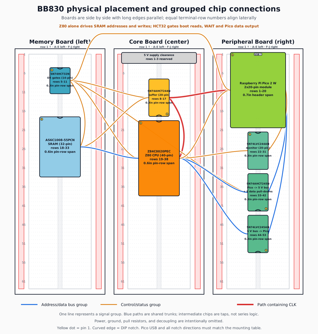
Memory uses 23 terminal rows for ICs, Core 30, and Peripheral 50. Leave gaps, keep bypass capacitors near supply pins, and place address pulls by the SRAM trunk and Pico data pulls beside U9/U10 A pins. No reset transistor is fitted.
Power Distribution
Feed the three +5 V rails from one supply-entry star, with multiple short common-GND links near bus crossings. The Peripheral +3.3 V rail is supplied only by Pico header 36 and powers U7/U10. Do not connect a plug-in module's 3.3 V output to it. Fit seven local 100 nF capacitors, three 22 uF board capacitors, and one 100 uF entry capacitor. Observe electrolytic polarity; the 1N5819 band faces VSYS.
All installed 5 V ICs must be powered whenever the 5 V rail is on. Pulls do not isolate installed unpowered devices. Follow Phase 0.
3.2 KiCad Electrical Schematic
The native schematic and net manifest are generated by build-kicad-schematic.py. Current validation: zero ERC violations, 71 real nets, 278 pin endpoints. This establishes connectivity, not bench timing or supply-transient safety.
The two PCB designs implement the same assisted-loader circuit with DIP / through-hole or partial-SMT assembly. Their packages, SRAM parts, placement and fabrication files differ. Follow the chosen board's mechanical checks and qualify its 20 MHz target independently; breadboard row positions do not apply to either PCB.