DIP / Through-Hole PCB Design Considerations
These constraints apply to hardware/kicad/. The
partial-SMT design has different packages,
placement, SRAM timing and assembly requirements.
Revision B is a compact 85 x 96 mm implementation of the current eight-package assisted-loader circuit. It retains the IC set already tested at 20 MHz on the project prototype. 20 MHz is this layout's qualification target, not a measured result for an assembled PCB.
Layer stack and routing rules
| Layer | Role |
|---|---|
| F.Cu | Signals, locked via-free clock preroutes |
| In1.Cu | Solid GND plane; no signal tracks |
| In2.Cu | Solid +5V power plane; no signal tracks |
| B.Cu | Signals |
The generator writes this 1.6 mm stack-up into the board file:
| Layer | Material | Thickness |
|---|---|---|
| F.Cu | Copper | 0.035 mm |
| Prepreg | 7628, Er 4.4 | 0.2104 mm |
| In1.Cu | Copper (GND) | 0.0152 mm |
| Core | FR-4, Er 4.4 | 1.065 mm |
| In2.Cu | Copper (+5V) | 0.0152 mm |
| Prepreg | 7628, Er 4.4 | 0.2104 mm |
| B.Cu | Copper | 0.035 mm |
This is a common 1.6 mm JLC-style four-layer stack; confirm the fabricator's actual stack before ordering. Every signal layer sits about 0.21 mm from a solid plane: F.Cu references GND and B.Cu references +5V. The planes are separated by the 1.065 mm core. 100 nF bypass capacitors and the through-hole pins on both planes tie the +5V plane to GND, so it acts as an AC reference for B.Cu. Through-hole GND and +5V pads connect to their planes with thermal reliefs. Both planes are voided around the antenna cutout; do not route signals across that void.
Signals are 0.30 mm, power 0.60 mm, with 0.20 mm default clearance. Clock clearance is 0.30 mm. That is 50% above the default, and it still lets a 0.30 mm clock track pass between adjacent DIP pins: the 1.6 mm pads leave 0.94 mm, and 0.30 + 2 x 0.30 = 0.90 mm. A 0.40 mm clearance would block those channels and force much longer clock detours around package ends. The router uses an additional 0.01 mm signal clearance margin to avoid rounding failures on imported diagonals. No DRC warning is waived to accept the route.
Placement and mechanical clearance
The Pico lies horizontally at the upper left. The Z80 (U1) and SRAM (U2) are parallel horizontal packages in the lower half. U4 (AHCT244) and U3 (HCT32) stand vertically at their left ends, keeping the Z80 clock, CE#, WAIT# and RD# paths short. U9/U10 share the data bus beside the Pico. RN5/RN6 are local to the startup GPIOs. The +5V bypass capacitors are 2.9-5.9 mm from their supply pins across the +5V plane. The +3V3 bypass tracks for U7 and U10 are 6.1 and 5.0 mm, via-free. Each capacitor's other pad joins the GND plane.
Four 2.7 mm non-plated holes accept M2.5 standoffs, one in each corner, with centres 4 mm from both adjacent edges:
| Corner | Centre relative to the upper-left board edge |
|---|---|
| Upper left | 4, 4 mm |
| Upper right | 81, 4 mm |
| Lower right | 81, 92 mm |
| Lower left | 4, 92 mm |
Hole spacing is 77 x 88 mm. The mounting footprints reserve a 5.9 mm courtyard around a nominal 5.4 mm hardware envelope; use hardware no wider than 5.4 mm overall. Check enclosure bosses, underside lead lengths and standoff height before assembly. Package courtyards are not a guarantee of purchased socket-body fit.
The Pico USB faces outward at the left edge. Its official antenna keepout is inside a chamfered FR-4/copper cutout that clears the keepout by about 0.3 mm on the long sides and 1.3-1.5 mm at the ends. The Pico header pads beside the cutout keep about 0.7 mm of copper-to-edge clearance for milling tolerance. Keep antenna space clear of metal, wiring and enclosure walls; geometry alone does not qualify Wi-Fi.
OLED mounting
A2 reserves the complete 38 x 12 mm OLED body at the upper right, with 0.5 mm assembly courtyard around it. The module drawing locates the header 1.50 mm from the left edge and SDA 2.19 mm from the top, with 2.54 mm pitch. The socket order, bottom-to-top viewed from above, is GND, VCC, SCK/SCL, SDA. VCC is 3.3 V, SCL is GP26 and SDA is GP22.
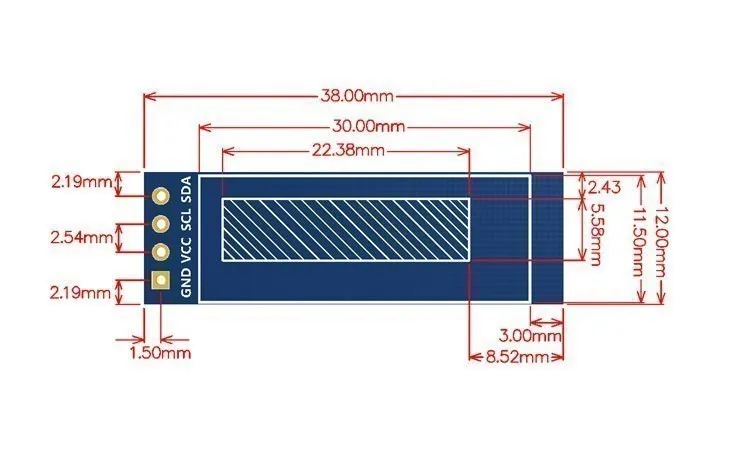
Use a 1x4 female socket and an insulating support at the far end. The carrier drills are 1.0 mm: verify the selected socket tail diameter. The drawing does not dimension module mounting holes or assembled height; do not drill invented holes or assume the display is supported by its pins alone. The 3D preview does not include an OLED or socket model.
USB-C power module mounting
J1 uses the pictured 21.6 x 12.7 mm breakout, mounted at the top edge with USB-C facing outward. Solder all six 2.54 mm header pins to the module and to the carrier's 1.0 mm plated holes. The pad order in the photograph is CC2, D+, D-, CC1, GND, VBUS. Only VBUS and GND connect to main-board nets; all four other pads remain isolated.

The six soldered pins secure the module without screw holes. The fabrication outline is scaled from the vendor dimension photograph. The pin row is centred on the module's long edge, 1.36 mm from its rear edge. The body ends at the board's top edge, and the USB-C shell overhangs it by about 1.5 mm. The courtyard is flush with the top edge. Dry-fit the purchased module before fabrication: the outline comes from a photo, not a mechanical drawing. Check pin fit, cable access and insulating underside clearance. Avoid cable loads on the six joints; no insertion-force qualification is claimed. The 3D preview does not include this breakout.
Power and startup safety
J1 supplies +5 V directly from a regulated 5 V USB source; it is not a regulator or a USB-PD trigger. Verify the breakout's two 5.1 kOhm CC sink resistors before USB-C-to-USB-C use. J3 remains an optional auxiliary input/probe header: pin 1 +5 V, pin 2 GND. J1 and J3 share the same rail without source isolation: use only one supply at a time. D1 feeds Pico VSYS, never Pico VBUS. The +5V input has no reverse-polarity diode or polyfuse; the prototype-proven circuit is kept unchanged. Use a regulated, current-limited 5 V source. Pico's 3.3 V output is the only source for U7/U10 and the OLED.
Power sequencing
Apply J1 power (or J3 power, not both) before connecting Pico USB. Disconnect Pico USB before removing main power. AHCT245 data pins lack power-off isolation. USB-only operation/programming of the populated board is unsupported; the VSYS diode does not isolate GPIOs. All installed 5 V ICs must be powered together.
Six bussed resistor arrays implement all 40 independent 10 kOhm pull branches. Their common pins connect only to their specified rails. RN5 replaces breadboard R17-R20; RN6 replaces R21-R24. No resistor joins two signal branches together. Both data paths default disabled, boot-read inhibit defaults HIGH, and clock/reset/bank-select/I/O-release default LOW.
Retain the polarized C8-C11 markings and D1's cathode band toward VSYS. Supply-entry capacitance does not replace the seven local bypass capacitors.
Trace lengths and signal synchronisation
The machine-readable route report records total copper, longest pad path, vias, source-specific paths and layer changes. These are planar copper lengths, not measured electrical flight times; layer changes include transitions through plated component pads.
| Source/receiver group | Path range | Spread |
|---|---|---|
| Z80 to SRAM address | 11.46-54.81 mm | 43.36 mm |
| Z80 to SRAM data | 27.50-61.02 mm | 33.51 mm |
| Pico-write transceiver to SRAM | 38.58-75.17 mm | 36.59 mm |
| SRAM to Pico-read transceiver | 52.57-81.35 mm | 28.79 mm |
| Pico to U9 | 10.56-73.73 mm | 63.18 mm |
| Pico to U10 | 21.68-70.97 mm | 49.29 mm |
Using an illustrative FR-4 delay of 6-7 ps/mm, the address spread corresponds to about 0.26-0.30 ns, and the CPU/SRAM data spread to 0.20-0.23 ns. These estimates are small compared with the 50 ns period at 20 MHz, but do not establish setup/hold margin. Do not add serpentine copper simply to match bus totals: each shared branch affects multiple source/receiver paths. A0-A7 are short direct Z80-to-SRAM runs.
| Critical driven path | Length | Layer changes |
|---|---|---|
| Pico clock to U4 | 53.20 mm | 0 |
| U4 to Z80 clock | 36.55 mm | 0 |
| U4 to SRAM CE# | 18.38 mm | 0 |
| U3 to SRAM OE# | 50.38 mm | 0 |
| U4 to SRAM WE# | 44.26 mm | 0 |
| U3 to Z80 WAIT# | 39.03 mm | 1 |
| Z80 IORQ# to U3 | 34.78 mm | 1 |
| Z80 RD# to U4 | 30.46 mm | 0 |
| Buffered RD# U4 to U3 | 24.17 mm | 0 |
| U4 to SRAM A16 | 48.55 mm | 0 |
Both clock nets are locked, via-free F.Cu preroutes. The Pico clock daisy-chains through its RN6 pull-down to U4 with no stub. The Z80 clock is a direct U4-to-CPU route. The board has no test points; the circuit is proven on the prototype, so probe IC pins or socket leads directly.
SRAM CE#, OE# and WE# are via-free. The SRAM-to-Pico-read-transceiver paths are the remaining outliers (D3 at 81 mm; D1 with four layer changes); check them at the U10 receive pins before accepting 20 MHz operation. No route is claimed to be length matched.
Timing and hardware qualification
Do not equate 55 ns SRAM access time with a complete memory transaction, or assume one 50 ns clock period is the entire Z80 read window. Check the actual M1/memory-read sampling edges against address-valid time, AHCT244/HCT32 propagation, SRAM CE#/OE#/access times, CPU setup/hold, and PCB delay. Check write pulse width and address/data setup/hold independently.
Start at 1 MHz on the PCB, then qualify increasing rates through 20 MHz. Reuse applicable frequency tests and record results separately from the prototype: cold boots, SRAM patterns in both banks, bank switching, reset/load/recovery, I/O WAIT and clock stop/ resume, CP/M disk traffic, and sustained network/USB operation.
Use the DHO814 for receive-pin levels, edge quality, clock duty/pulse width, overshoot, ringing and timing margin. Use the DSLogic Plus groups for bus ordering. Neither DRC, a render nor a terminal session establishes these properties.