DIP / Through-Hole PCB
This page covers the DIP / through-hole design in hardware/kicad/.
For the other design, see the partial-SMT PCB, or
compare both boards. This is the budget-oriented option
for one hand-built machine: populate one board from the bare-PCB batch
without paying for factory assembly.
The PCB is a separate physical implementation of the Z80 ROMless SBC: a 85 x 96 mm, four-layer, through-hole board implementing the current eight-package assisted-loader circuit. It includes a socket and full body reservation for the 38 x 12 mm OLED, six resistor arrays for all 40 pull branches, and four corner M2.5 standoff holes. The USB-C power breakout mounts directly on the PCB using six soldered pins.
The IC set is shared with the 20 MHz prototype. The PCB targets 20 MHz and has its own routing measurements and qualification requirements. Matching electrical connectivity does not establish physical operation.
The Phase 0-10 implementation plan remains the three-BB830 breadboard build. Do not use its socket-row positions or incremental jumper-wiring instructions as PCB assembly instructions.
| Page | Covers |
|---|---|
| PCB inventory | PCB-specific fitted parts, sockets, connectors, mechanical items, and differences from the breadboard BOM |
| Design considerations | Layer stack, component placement, power sequencing, routing, timing, and assembly constraints |
| Shared electrical reference | Exact IC pin assignments and SRAM-control logic |
| Shared Pico firmware | Phase programs, CP/M images and Pico provisioning; PCB qualification is separate |
Board preview
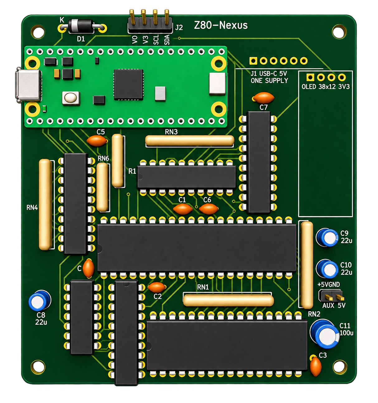
Preview exported from the current KiCad layout and enhanced using ChatGPT. Click to enlarge it. IC and Pico models are shown, but socket, OLED, USB-C breakout and standoff models are not included. The render does not establish physical assembly clearance.
Design status and boundaries
The schematic has 30 components, 71 real nets and 278 connected pin endpoints, excluding the ERC-only power marker. All 30 schematic footprints and 278 connected endpoints are on the PCB, including the onboard J1 USB-C power breakout. Its other four pins have isolated solder pads, not signal connections. Revision B has no test points: the circuit is proven on the prototype, so probe IC pins or socket leads directly. Four 2.7 mm NPTH mounting footprints are additional mechanical features. The corner holes are 4 mm from both adjacent edges, with 77 x 88 mm centre spacing for four M2.5 standoffs.
The routed PCB and its fabrication files have passed the repository's connectivity, layout, and generation checks. This is not a hardware-qualified design. Start physical bring-up at 1 MHz. Qualification through 20 MHz is the PCB design target, not a demonstrated operating speed for this board.
Electrical requirements and applicable firmware tests are shared, but PCB assembly and qualification records must be separate. A passing breadboard does not qualify the PCB, and a clean PCB does not qualify the breadboard. An independently documented PCB assembly/bring-up sequence and measured timing evidence are still required before claiming a working hardware build.
Editable sources and drawings
Paths below are relative to the repository root.
| Artifact | Purpose |
|---|---|
| KiCad project | Project configuration and design rules |
| Native schematic | Electrical connections and fitted component values |
| Routed PCB | Editable placement, copper, outline, and silkscreen |
| Schematic PDF | Full electrical drawing |
| PCB SVG / PDF | Copper, silkscreen, and outline drawings |
| Board preview | 3D board rendering; absent component/socket models cannot establish assembly clearance |
| DRC report / board statistics | Generated layout evidence |


Source ownership and regeneration
The schematic generator, scripts/build-kicad-schematic.py, owns component
values, exact pin/net assignments, symbols, and the net manifest.
scripts/build-kicad-pcb.py owns placement, board geometry, netclasses,
silkscreen, GND/+5V plane and stack-up setup, and PCB invariants.
The normalized unrouted input is
hardware/kicad/reports/z80_romless_sbc.dsn; the accepted routing session is
hardware/kicad/reports/z80_romless_sbc.ses. Regeneration must reproduce that
session's exact copper, not silently substitute an independently edited route.
Follow the checkout's
KiCad generation instructions.
Keep the project closed while generating or replacing its files. The separate
router image is built from scripts/freerouting/Containerfile; it uses
checksum-pinned Freerouting and Java with network access disabled during
routing. No separate checkout is needed.
Before accepting regenerated outputs, require zero ERC violations, zero DRC violations and unconnected items, matching pin/net and component-value manifests, and matching routing-session copper. Publish the drawings, BOM, and fabrication package together only after these gates pass.
Fabrication package
The manufacturing outputs are under hardware/kicad/fabrication/.
| Artifact | Purpose |
|---|---|
| Gerber/drill ZIP | Copper, mask, silkscreen, board edges, and plated/non-plated drills |
| Generated BOM | Authoritative fitted component references, values, and footprints |
| Placement CSV | Through-hole component positions |
| IPC-D-356 netlist | Electrical manufacturing-test netlist |
Use a four-layer, 1.6 mm FR-4 fabrication stack with plated through holes and both solder masks. Confirm the manufacturer's actual stack-up, internal cutout process, and drill capabilities before ordering. Review the inventory against purchased parts and the mechanical constraints; the generated files alone do not establish that every purchased socket or component fits.