DIP / Through-Hole PCB Inventory
These parts are for the DIP / through-hole PCB, not the partial-SMT inventory. See Choose a PCB design before buying parts or ordering boards.
This is the Revision B 85 x 96 mm, four-layer assisted-loader PCB. The generated BOM owns fitted references, values and footprints. Sockets, standoffs and module pin headers are additional assembly/purchase items.
Semiconductors and sockets
| Reference | Part | Socket/package |
|---|---|---|
| A1 | Raspberry Pi Pico 2 W | Two soldered 20-pin male headers and two 20-position socket strips |
| U1 | Z84C0020PEC | DIP-40, 15.24 mm socket |
| U2 | AS6C1008-55PCN | DIP-32, 15.24 mm socket; A16 is buffered bank select |
| U3 | SN74HCT32N | DIP-14, 7.62 mm socket |
| U4 | SN74AHCT244N | DIP-20, 7.62 mm socket |
| U7 | SN74LVC244AN | DIP-20, 7.62 mm socket |
| U9 | SN74AHCT245N | DIP-20, 7.62 mm socket |
| U10 | SN74LVC245AN | DIP-20, 7.62 mm socket |
| D1 | 1N5819 | DO-41 axial, 10.16 mm pitch; cathode band toward VSYS |
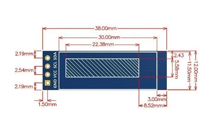
| A2 | 0.91-inch SSD1315 128x32 I2C OLED | 38 x 12 mm body, 1x4 2.54 mm female socket; 3.3 V |
The eight core active packages are A1 and seven DIP ICs; A2 is the additional display. Buy four DIP-20 sockets, one DIP-14, one DIP-32 and one DIP-40. Do not interchange AHCT, HCT and LVC families. Verify actual socket-body dimensions and extraction access, not just pin-row spacing.
The silkscreen inside each DIP outline names the chip with its reference underneath, for example 74AHCT245 / U9 and Z80 CPU / U1. Check the label before fitting the socket and chip, because the fitted part covers it.
Resistor arrays
All 40 pull branches use six bussed arrays, with no discrete resistors fitted on the PCB.
| References | Qty | Value/package | Purpose/common pin |
|---|---|---|---|
| RN1, RN2 | 2 | 8x10 kOhm bussed, SIP-9 | A0-A15 pull-ups; pin 1 +5 V |
| RN3 | 1 | 8x10 kOhm bussed, SIP-9 | Pico D0-D7 pull-downs; pin 1 GND |
| RN4 | 1 | 8x10 kOhm bussed, SIP-9 | Eight CPU control pull-ups; pin 1 +5 V |
| RN5 | 1 | 4x10 kOhm bussed, SIP-5 | GP4/5/6/7 startup pull-ups; pin 1 3.3 V |
| RN6 | 1 | 4x10 kOhm bussed, SIP-5 | GP2/3/9/8 startup pull-downs; pin 1 GND |
Use bussed, not isolated, networks. Verify the common-pin marking and 2.54 mm pitch. RN5 implements breadboard R17-R20 in order; RN6 implements R21-R24 in order. Never fit the corresponding discrete resistors as well. The breadboard inventory still specifies 40 individual resistors for breadboard construction.
Capacitors
| References | Qty | Value | Footprint/rating |
|---|---|---|---|
| C1-C7 | 7 | 100 nF | Ceramic disc or monolithic, 2.50-2.54 mm pitch, body up to 5 mm, at least 10 V |
| C8-C10 | 3 | 22 uF | 4 mm radial electrolytic, 2.00 mm pitch, at least 10 V (16 V recommended) |
| C11 | 1 | 100 uF | 6.3 mm radial electrolytic, 2.50 mm pitch, at least 10 V (16 V recommended) |
C8-C11 positive pad 1 is +5 V and negative pad 2 is GND. Retain polarity silkscreen. The silkscreen marks each electrolytic with its value (22u or 100u) under the reference. Confirm purchased body diameters and lead pitches.
Connectors, display and mechanical hardware
| Item | Qty | Requirement |
|---|---|---|
| J1 USB-C power breakout | 1 | Pictured 21.6 x 12.7 mm module; all six pins soldered, only VBUS/+5 V and GND connected |
| J1 male pin strip | 1 | 1x6, 2.54 mm; solder to module and carrier, 1.0 mm carrier drills; verify pin fit and underside insulation |
| J3 auxiliary power/probe header | 1 | 1x2, 2.54 mm: pin 1 +5 V, pin 2 GND; use only one source, J1 or J3 |
| J2 expansion header | 1 | 1x4, 2.54 mm: GP22/SDA, GP26/SCL, 3.3 V, GND; silkscreen pin labels SDA, SCL, 3V3, GND |
| OLED female socket | 1 | 1x4, 2.54 mm; 1.0 mm carrier drills, verify pin fit |
| OLED insulating support | 1 | Support module's far end; determine height with the purchased socket/module |
| PCB | 1 | Four-layer, 1.6 mm FR-4 (GND and +5V inner planes), 85 x 96 mm, internal antenna cutout |
| M2.5 standoffs and fasteners | 4 sets | Four corner 2.7 mm NPTH holes, 77 x 88 mm spacing; hardware no wider than 5.4 mm overall, 5.9 mm courtyard |
Use the pictured USB-C module, not the different 12 x 13.8 mm part description. Viewed as photographed with USB-C at the top, the six pads are CC2, D+, D-, CC1, GND, VBUS. The first four have isolated carrier pads: solder them for support but do not wire them to main-board nets. The breakout itself must retain its two 5.1 kOhm CC sink resistors. No module screw fixings are required.

The OLED socket order is GND, VCC, SCK/SCL, SDA, bottom-to-top viewed from above. Its body/connector position follows the dimension drawing. No module mounting-hole dimensions or assembled-height dimensions are given. Do not assume the board render includes socket, OLED, USB-C breakout or standoff models.
Use a regulated +5 V supply rated at least 1 A, preferably current limited. Apply main power before connecting Pico USB and disconnect Pico USB first. J1 and J3 are not isolated from each other: do not connect both supplies. Do not power the populated board from Pico USB alone. See power and startup safety. No PLD programmer is required. Reuse the shared multimeter, oscilloscope and logic-analyzer equipment for PCB-specific qualification through the 20 MHz target.