Partial-SMT PCB
This is the 98.3 x 60 mm, four-layer design in hardware/kicad-smt/.
JLCPCB assembles the top-side surface-mount parts, including the Pico 2 W.
The Z80, OLED socket and J2/J3 headers are hand-soldered.
For a single machine with lower assembly outlay and socketed ICs, consider the DIP / through-hole PCB. See Choose a PCB design for the assembly and cost comparison.
| Page | Covers |
|---|---|
| Inventory and assembly | Exact SMT parts and LCSC numbers, passives and the four hand-fitted items |
| Design considerations | Replacement SRAM, layout, power sequencing, mechanical fit and placement-preview checks |
| Shared pin map | Signal connections and SRAM-control logic; use the SMT inventory for package suffixes |
| Shared firmware | Pico firmware and CP/M provisioning; physical qualification remains board-specific |
Board preview
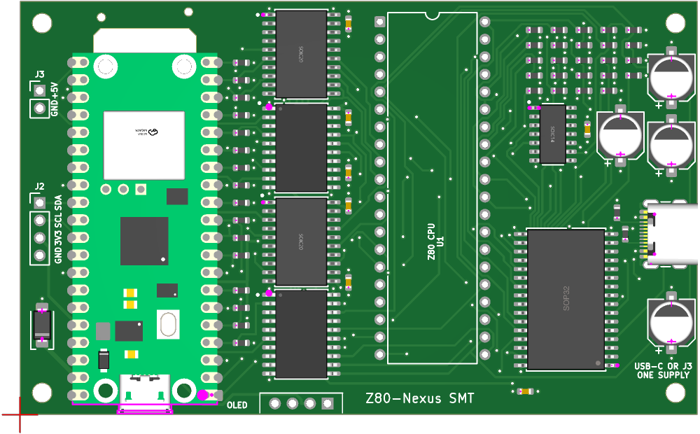
Exported from the SMT KiCad layout. Models illustrate placement but do not prove purchased-part fit, connector clearance or assembled height.
Design status and boundaries
The SMT schematic has 66 components, 73 real nets and 325 connected endpoints, excluding ERC-only power markers. The PCB includes those 66 footprints and four additional mechanical mounting-hole footprints. The assembly BOM includes 62 JLC-assembled parts; U1, A2, J2 and J3 are intentionally absent from the JLC BOM and placement file.
The schematic and routed board pass the maintained connectivity, ERC/DRC and generation checks. This is not hardware qualification. Start assembled-board bring-up at 1 MHz and qualify the 20 MHz target separately. The breadboard's CPU/SRAM-absent stages cannot be applied unchanged to a board with factory-soldered SRAM and logic.
Editable sources and drawings
| Artifact | Purpose |
|---|---|
| KiCad project | SMT design rules and project configuration |
| Native schematic | Exact connections, parts and LCSC numbers |
| Routed PCB | SMT placement, copper, outline and silkscreen |
| Schematic PDF | Electrical drawing |
| PCB SVG / PDF | Layer and assembly drawings |
| ERC report / DRC report | Generated electrical and layout checks |

Source ownership and regeneration
scripts/build-kicad-smt-schematic.py owns the schematic, symbols, exact
pin/net assignments, component details and manifest.
scripts/build-kicad-smt-pcb.py owns the SMT placement, geometry, rules,
keepouts, models and board checks. scripts/export-jlc-assembly.py
generates the JLC BOM and component placement list (CPL).
The accepted route is
hardware/kicad-smt/reports/z80_romless_sbc_smt.ses; its normalized
unrouted input is z80_romless_sbc_smt.dsn in the same directory.
Do not substitute files from the DIP project.
With the project saved and closed in KiCad, run from the repository root:
PYTHON=.venv-kicad/bin/python npm run kicad:smt
Follow the SMT project build instructions
for prerequisites. The pipeline checks ERC, manifest parity, PCB/DSN
reproduction, zone-refilled DRC, route budgets, solder-mask/silkscreen
clearances and JLC BOM/CPL consistency before publishing the outputs.
It does not modify the DIP project in hardware/kicad/.
Fabrication and assembly files
All files in this table belong to the SMT design.
| File | Use |
|---|---|
| Gerber/drill ZIP | Upload for the PCB order |
| JLC assembly BOM | Upload as the PCBA BOM |
| JLC CPL | Upload as the PCBA component placement file |
| Full BOM | Purchase/assembly reference including hand-soldered parts; not the JLC upload BOM |
| KiCad positions | Complete placement reference; use the corrected JLC CPL for PCBA |
| IPC-D-356 netlist | Electrical manufacturing-test netlist |
The ZIP contains four copper layers, front paste, both solder masks and silkscreens, the outline/antenna window, job file and separate plated and non-plated drill files.
JLCPCB order settings
- PCB: FR-4, four layers, 1.6 mm, 98.3 x 60 mm.
- Layer order: front, GND, +5V, back; 1 oz outer and 0.5 oz inner copper.
- Finish: LeadFree HASL, green solder mask and white silkscreen.
- Cutout: enclosed Pico antenna window, with the top FR-4 bridge retained.
- PCBA: top side only, Economic PCBA. The board's 60 mm height is below the 70 x 70 mm single-board minimum for Standard PCBA; Standard would require a panel with edge rails and fiducials.
- Upload the matching SMT ZIP, JLC BOM and JLC CPL, then review every component's rotation and polarity.
- Check current part availability and any required Pico 2 W X-ray inspection in the quote. Pre-order the module into your JLC parts library if necessary.
The five-board bare-PCB batch and the PCBA assembly quantity are separate; check both in the quote. Include assembly and component-loading charges when comparing this option with one hand-built DIP machine.